In recent years, with the continuous reduction of chip size, the short channel effect and thermal effect have become more and more obvious. The development of a new two-dimensional quantum material system to achieve transformative device applications has become a research hotspot in current science and technology. Large-scale high-end device applications must be based on large-area, high-quality single crystal materials, so the preparation and research of two-dimensional single crystal materials has important scientific significance and technical value. As the only two-dimensional semiconductor without dangling bonds, the preparation of large-area single crystals of hexagonal boron nitride has always been a bottleneck that is difficult to break through in this field. The main problem is the twin grain boundaries generated during the epitaxial growth process: that is, when the crystal domains have two dominant orientations with an angle of 180° on the conventional single crystal substrate, the reverse crystal domains will form defect grain boundaries when they are spliced. . This problem is common in the preparation of most two-dimensional material single crystals, so the research on the preparation of hexagonal boron nitride single crystal materials has very important scientific significance and technical value.
Recently, Academician Wang Enge, Academician Yu Dapeng, Researcher Liu Kaihui of Peking University and their collaborators realized the epitaxial preparation of decimeter-scale two-dimensional single-crystal hexagonal boron nitride on a single-crystal copper substrate with broken central inversion symmetry. The mechanism is given a detailed experimental and theoretical analysis. The relevant results were published in the journal Nature under the title of "Epitaxial growth of a 100-square-centimetre single-crystal hexagonal boron nitride monolayer on copper".
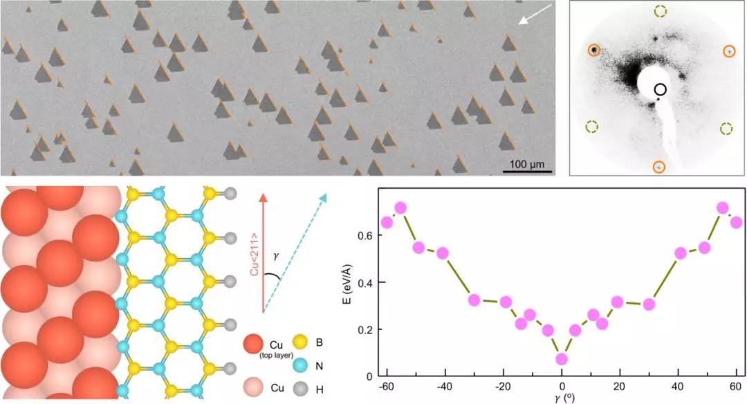
After repeated research, the research team has explored a new method of using symmetry-broken substrate epitaxy to invert symmetric two-dimensional single-crystal thin films. This method converts industrial polycrystalline copper foil into copper (110) small-angle tilted crystal plane with only C1 symmetry through a patent-protected annealing process, using the unique Cu<211> steps and hexagonal boron nitride crystals on this crystal plane The difference in coupling strength between the boron-type and nitrogen-type zigzag boundaries of domains breaks the degeneracy of domain orientation during the growth of hexagonal boron nitride, thereby achieving domain growth with consistent orientation and seamlessly splicing into a two-dimensional single-crystal film. This method can be extended to the preparation of large-area single crystals of other two-dimensional materials, and is expected to promote the technical development of large-scale application of new two-dimensional material devices.

Epitaxial preparation and growth mechanism of two-dimensional single crystal hexagonal boron nitride